
新闻中芯
新闻中芯
05
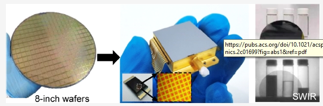
2024.12Wafer-Scale Fabrication of CMOS-Compatible Trapping-Mode Infrared Imagers with Colloidal Quantum Dots
Silicon-based complementary metal oxide semiconductor (CMOS) devices have dominated the technological revolution in the past decades. With increasing demands in machine vision, autonomous driving, and artificial intelligence, silicon CMOS imagers, as the major optical information input devices, face great challenges in spectral sensing ranges. In this paper, we demonstrate the development of CMOS-compatible infrared colloidal quantum-dot (CQD) imagers in the broadband short-wave and mid-wave infrared ranges (SWIR and MWIR, 1.5−5 μm). A new device architecture of trapping-mode detectors is proposed, fabricated, and demonstrated with lowered darkcurrents and improved responsivity. The CMOS-compatible fabrication process is completed with two-step sequential spin-coating processes of intrinsic and doped HgTe CQDs on an 8 in. CMOS readout wafer with photoresponse non-uniformity (PRNU) down to 4%, dead pixel rate of 0%, external quantum efficiency up to 175%, and detectivity as high as 2 × 10¹¹ Jones for extended SWIR at 300 K and 8 × 10¹⁰ Jones for MWIR at 80 K. Both SWIR images and MWIR thermal images are demonstrated with great potential for semiconductor inspection, chemical identification, and temperature monitoring.
了解详情
05
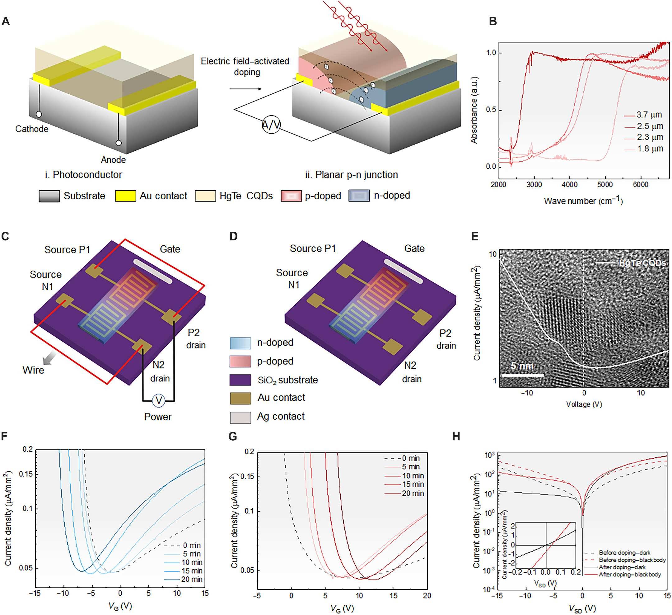
2024.12Mercury telluride colloidal quantum-dot focal plane array with planar p-n junctions enabled by in situ electric field–activated doping
Colloidal quantum dot (CQD)–based photodetectors are promising alternatives to bulk semiconductor-based detectors to be monolithically integrated with complementary metal-oxide semiconductor readout integrated circuits avoiding high-cost epitaxial growth methods and complicated flip-bonding processes. To date, photovoltaic (PV) single-pixel detectors have led to the best performance with background-limit infrared photodetection performance. However, the nonuniform and uncontrollable doping methods and complex device configuration restrict the focal plane array (FPA) imagers to operate in PV mode. Here, we propose a controllable in situ electric field–activated doping method to construct lateral p-n junctions in the short-wave infrared (SWIR) mercury telluride (HgTe) CQD–based photodetectors with a simple planar configuration. The planar p-n junction FPA imagers with 640 × 512 pixels (15-μm pixel pitch) are fabricated and exhibit substantially improved performance compared with photoconductor imagers before activation. High-resolution SWIR infrared imaging is demonstrated with great potential for various applications including semiconductor inspection, food safety, and chemical analysis.
了解详情
05
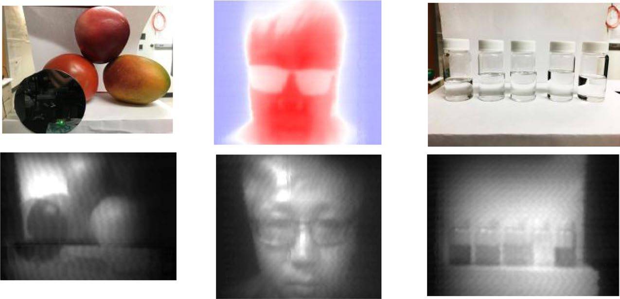
2024.12Dual-band infrared imaging using stacked colloidal quantum dot photodiodes
Infrared multispectral imaging is attracting great interest with the increasing demand for sensitive, low-cost and scalable devices that can distinguish coincident spectral information. However, the widespread use of such detectors is still limited by the high cost of epitaxial semiconductors. In contrast, the solution processability and wide spectral tunability of colloidal quantum dots (CQDs) have inspired various inexpensive, high-performance optoelectronic devices. Here, we demonstrate a twoterminal CQD dual-band detector, which provides a bias-switchable spectral response in two distinct bands. A vertical stack of two rectifying junctions in a back-to-back diode configuration is created by engineering a strong and spatially stable doping process. By controlling the bias polarity and magnitude, the detector can be rapidly switched between short-wave infrared and mid-wave infrared at modulation frequencies up to 100 kHz with D* above 1010 jones at cryogenic temperature. The detector performance is illustrated by dual-band infrared imaging and remote temperature monitoring.
了解详情
05
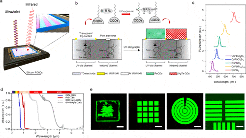
2024.12Direct Optical Lithography Enabled Multispectral Colloidal Quantum-Dot Imagers from Ultraviolet to Short-Wave Infrared
Complementary metal oxide semiconductor (CMOS) silicon sensors play a central role in optoelectronics with widespread applications from small cell phone cameras to large-format imagers for remote sensing. Despite numerous advantages, their sensing ranges are limited within the visible (0.4−0.7 μm) and near-infrared (0.8−1.1 μm) range , defined by their energy gaps (1.1 eV). However, below or above that spectral range, ultraviolet (UV) and short-wave infrared (SWIR) have been demonstrated in numerous applications such as fingerprint identification, night vision, and composition analysis. In this work, we demonstrate the implementation of multispectral broadband CMOS-compatible imagers with UV-enhanced visible pixels and SWIR pixels by layer-by-layer direct optical lithography of colloidal quantum dots (CQDs). High-resolution single-color images and merged multispectral images were obtained by using one imager. The photoresponse nonuniformity (PRNU) is below 5% with a 0% dead pixel rate and room-temperature responsivities of 0.25 A/W at 300 nm, 0.4 A/W at 750 nm, and 0.25 A/W at 2.0 μm.
了解详情
05
2024.12Megapixel large-format colloidal quantum-dot infrared imagers with resonant-cavity enhanced photoresponse
Infrared imaging is extensively explored due to its unique properties of high atmospheric transmission and temperature-dependent emission. Unfortunately, the current epitaxial infrared materials suffer from a complicated fabrication process and low production yield, which hinders the further development of infrared imaging for civilian applications. As an alternative to epitaxial semiconductors, the wide spectral tunability and optical versatility of colloidal quantum dots (CQDs) have provided a promising route for infrared detection. Here, we demonstrate an infrared imager that integrates HgTe CQDs with complementary metal-oxide-semiconductor (CMOS) readout integrated circuits. Moreover, the underlying metal contacts and passivation layer of the CMOS chip play a role as an in-pixel resonant-cavity , which enhances the absorption of the CQDs film. The CQDs imager exhibits a detectivity of 2.8 × 10¹⁰ Jones, an external quantum efficiency of 14%, and an operable pixel factor of over 99.99% for a cut-off wavelength of around 2 μm at room-temperature. With a large-format (1280×1024 pixels2) and a small pixel pitch of 15 μm, the resolution of the imager can reach 40 line pairs per millimeter (lp/mm). The performance of the CQDs imager is demonstrated by infrared imaging. © 2023 Author(s). All article content, except where otherwise noted, is licensed under a Creative Commons Attribution (CC BY) license (http://creativecommons.org/licenses/by/4.0/).
了解详情


 联系电话:史经理:15910422846/ 关经理:13054290736/申经理:17610066231
 联系地址:北京市北京经济技术开发区(通州)经海七路10号院5号楼
 京ICP备2022008750号-1