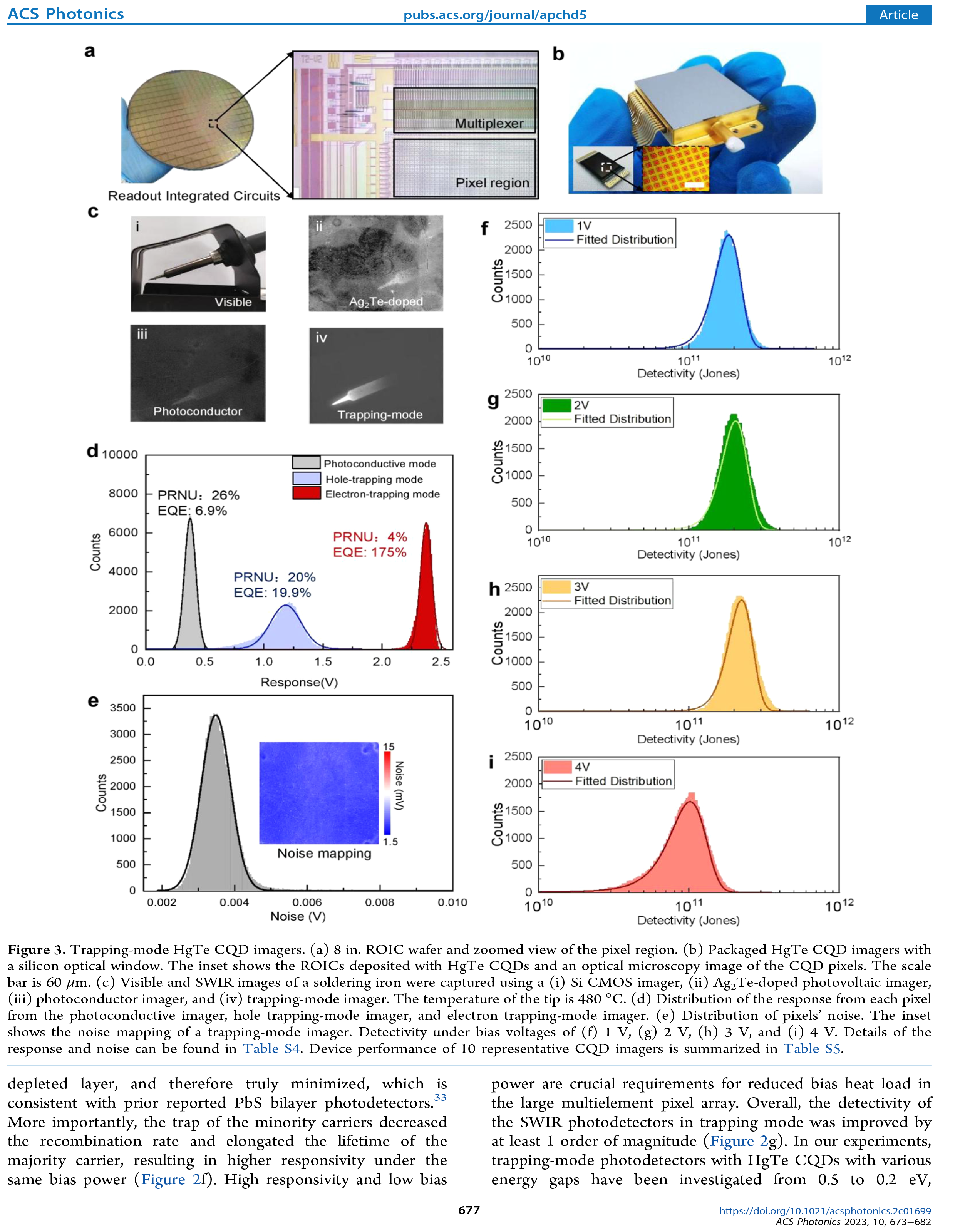
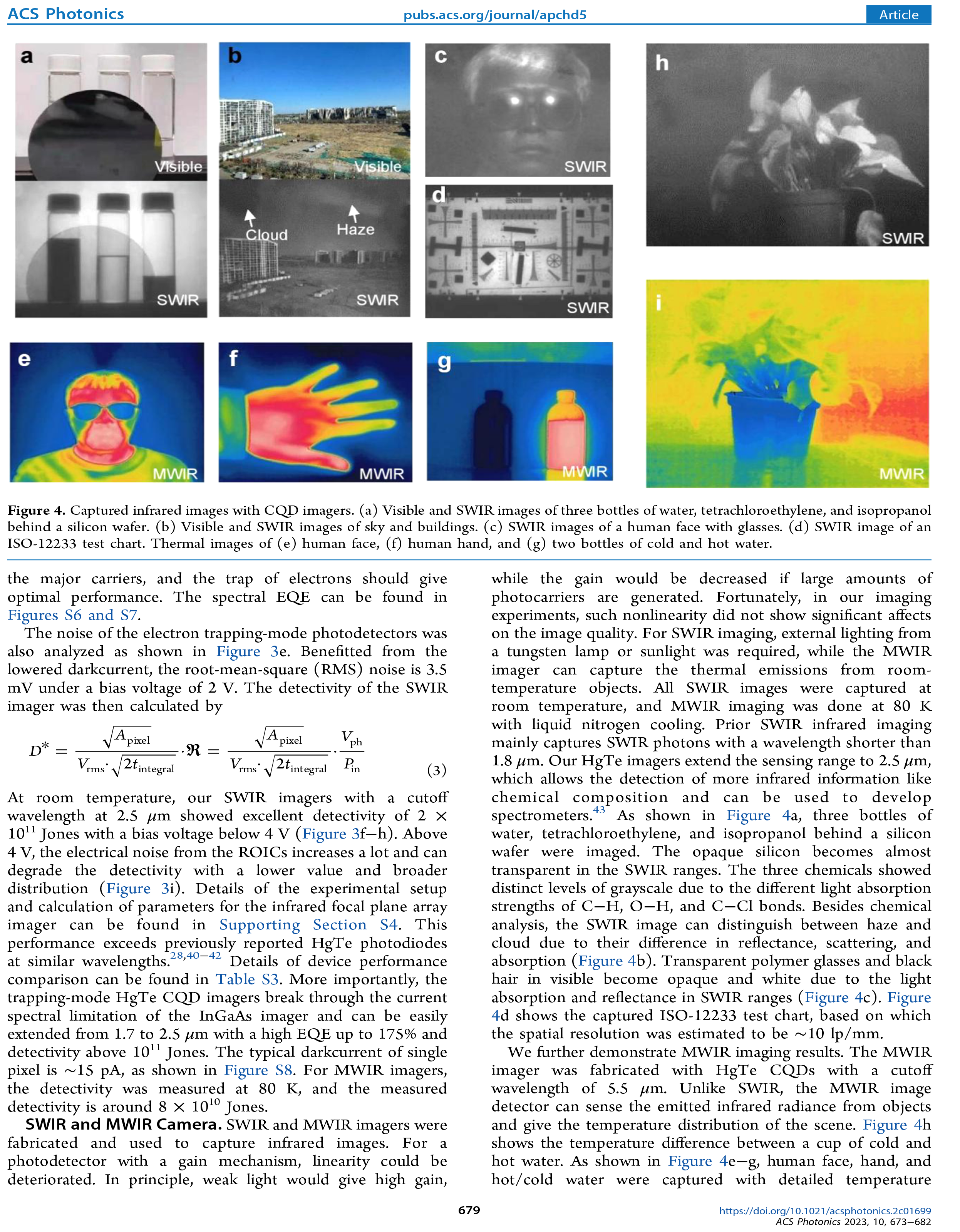
Wafer-Scale Fabrication of CMOS-Compatible Trapping-Mode Infrared Imagers with Colloidal Quantum Dots
2024.12.05


相关文章
- Mercury telluride colloidal quantum-dot focal plane array with planar p-n junctions enabled by in situ electric field–activated doping
- Dual-band infrared imaging using stacked colloidal quantum dot photodiodes
- Direct Optical Lithography Enabled Multispectral Colloidal Quantum-Dot Imagers from Ultraviolet to Short-Wave Infrared
- Megapixel large-format colloidal quantum-dot infrared imagers with resonant-cavity enhanced photoresponse


 联系电话:史经理:15910422846/ 关经理:13054290736/申经理:17610066231
 联系地址:北京市北京经济技术开发区(通州)经海七路10号院5号楼
 京ICP备2022008750号-1